Evaluate circuit material effects on PCB antenna PIM
In particular, as the number of wireless applications, wireless signals, and antennas grows, passive intermodulation (PIM) becomes an important performance parameter for PCB antennas, requiring an understanding of how different circuit material attributes can affect printed antenna PIM performance. PIM is a form of interference and is a circuit or system issue, and it is cautious to be aware that circuit materials can contribute to PIM issues. An educated choice of circuit material can pave the way for fabricating wireless PCB antennas with low levels of PIM that also meet their other antenna performance goals.
Many of the circuit material parameters important for active or passive circuits used at RF/microwave frequencies, such as dielectric constant (Dk), dissipation factor (Df), thermal conductivity, coefficient of thermal expansion (CTE), and thermal coefficient of dielectric constant (TCDk), can also provide insights into how well a circuit material will perform when used for a PCB antenna. Understanding what each parameter means in terms of antenna performance, along with how a circuit material can affect the PIM performance of a PCB antenna, can help guide the selection of antenna-grade circuit materials that will deliver predictable, dependable antenna performance.
Any choice of antenna-grade circuit material will start with Dk, with the value for a given circuit material an indication of the size of the circuit dimensions required for a particular wavelength and frequency. In general, materials with higher Dk values will support smaller antenna structures for a given frequency, although materials with lower Dk values typically support stronger and more consistent radiation patterns. The Dk consistency across a PCB material is one factor in achieving consistent and repeatable radiation patterns with a given printed antenna design, as is TCDk one barometer of how consistent PCB antenna performance will be with changes in temperature.
A circuit material’s TCDk parameter is typically referenced to room temperature (+25°C) and by how much the Dk changes at other temperatures. In terms of antenna performance, since a PCB antenna is designed to resonate within a particular frequency range, and the dimensions of its resonant structure are based on Dk, even moderate changes in Dk with temperature can result in variations in antenna frequency and radiation pattern.
Different circuit materials behave differently with changes in temperature. To demonstrate, Figure 1 plots Dk as a function of temperature for a number of circuit materials commonly used for high-frequency circuits, including PCB antennas. The circuit materials include polytetrafluoroethylene (PTFE) circuit materials with woven glass (WG) and ceramic fillers, low-cost FR-4, and three high-frequency circuit materials from Rogers Corp. (www.rogerscorp.com): RO3003™, RO4003C™, and RO4835™ circuit materials.

The Dk values of these materials are low, typically from about 2.1 through the thickness (z axis) of the material for PTFE-based circuit materials to about 4.8 for FR-4 circuit materials. As the plots of Dk with temperature show, the Dk values can change a great deal with temperature, resulting in circuit and antenna performance that will also change with temperature. For the RO3003, RO4003, and RO4835 materials, with Dk values ranging from 3.00 to 3.48 and held to a tolerance of ±0.05 or better across the circuit board, the changes with temperature are minimal, indicating that the impedances of circuit transmission lines and antenna traces will be consistent with temperature for consistent antenna performance with temperature.
Although circuit materials are readily available with higher values of Dk, circuit materials for PCB antennas generally exhibit a Dk of 3.5 or less through the material thickness when measured at 10 GHz. The use of a circuit material with lower Dk value allows for the use of wider conductors for a design frequency and for efficient radiation. One design goal for any PCB antenna is to minimize loss exhibited by the antenna circuitry as well as any loss when transferring high-frequency energy from the feedlines to a PCB antenna’s radiating elements. The use of circuit materials with Dk of about 3.5 or less promotes the design of efficient conductors. By selecting materials with low Df and smooth copper conductor surfaces for a PCB antenna, insertion losses can be minimized.
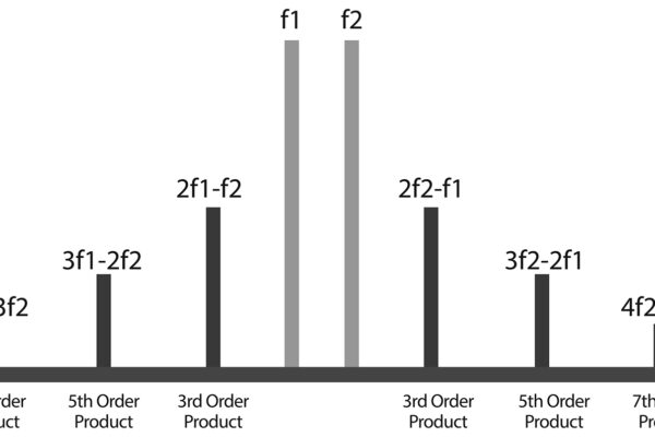
Intermodulation distortion, including PIM in passive PCB antennas, is of increasing concern with the growing numbers of wireless emitters. As Figure 2 shows, intermodulation results from the mixing of two or more closely located transmitted fundamental-frequency signals, f1 and f2, and their harmonics, 2f1, 2f2, 3f1, 3f2, and so on. The total of the coefficients of two mixing signals, such as 2f1 – f2 (2 and 1), determines the order of the resulting intermodulation product. As wireless services and their numbers of users increase, opportunities for intermodulation increase, with greater numbers of transmitted high-frequency signals. Intermodulation can occur in active circuits, such as frequency mixers or amplifiers, or as PIM in passive circuits, such as filters, couplers, and antennas.

Circuit materials and PIM
From Figure 2, it can be seen that PIM levels decrease with increasing order number, and that the third-order PIM products are usually of the greatest concern. Figure 2 does not show them, but even-order intermodulation products are also produced, and these can be a concern in some broadband applications. When the frequencies of any intermodulation products are within the frequency range of a nearby receiver, and the levels of the intermodulation products exceed the sensitivity of the receiver, they essentially function as noise to the receiver and can cause dropped calls, loss of data, and generally degraded wireless service.
While no circuit material is immune to the PIM of a passive circuit, such as a patch antenna, some circuit materials do better with PIM than others. PTFE-based high-frequency circuit materials have traditionally been known for low PIM levels, although such materials can require specialized processing steps and can be expensive choices for fabricating PCB antennas. Some non-PTFE-based thermoset circuit materials have fared well in PIM-sensitive designs, including as PCB antennas. Early concerns with the use of thermoset materials in such applications was that they lacked the low-loss (low Df) performance of PTFE-based circuit materials. But as the values in Table 1 show, a number of non-PTFE hydrocarbon circuit materials have been developed for PCB antennas with low Df loss and with PIM performance on par with PTFE-based circuit materials. The materials listed in Table 1 feature reasonably good TCDk values for stable performance with temperature, where |50| ppm/°C or less is considered good.

PIM can be caused by any number of variables in a system, including types of cables, loose connectors, and dirt on conductive surfaces. Materials with ferromagnetic properties are generally known to be potential sources of PIM. Ferromagnetic content of even 100 ppm or less in a dielectric material can elevate the PIM levels of a circuit material. For printed circuits, a number of factors can contribute to PIM performance, including the type of dielectric material, the quality of the etched circuitry, the quality of plated through holes (PTHs), the cleanliness of the PCB, soldermask, assembly issues, even the roughness of the copper conductor.
In fact, it is the surface roughness of the copper at the copper-substrate interface which has been found to be critical to PCB PIM performance. For the same material and transmission line, for example, smoother copper at this interface will result in lower levels of PIM. Table 2 lists the results of an internal study performed at Rogers Corp. which details the correlation between the root-mean-square (RMS) surface roughness of the copper at the copper-dielectric interface and the average PIM level. For the four items listed, the same substrate material, same dielectric thickness, same copper thickness, and same circuit design were used, with the only variation being the type of copper which had different amounts of surface roughness.

The treatment at the copper-substrate interface is not always considered in circuit material PIM studies, but it is generally not purely copper at that interface but a metal alloy used as a treatment to enhance the bond between the copper and the substrate material. The treatment also acts as a thermal barrier to the formation of copper oxide and to ensure good thermal robustness in the interface structure for the temperatures that will be used in processing the circuit material. While most copper treatments do not degrade PIM performance, some can and it must be considered as a possible factor that can contribute to circuit material PIM. For example, a nickel alloy copper treatment was found to have deleterious effects on PIM performance, since nickel is a ferromagnetic material.
Testing for PIM
As Table 2 indicates, small differences in versions of PCB materials can result in differences in PIM performance for printed antennas and other high-frequency circuits. With the low levels of PIM that are being evaluated, however, testing materials for PIM can be extremely challenging. No standard test method exists for evaluating circuit materials for PIM performance, although a test method has been developed at Rogers Corp. using a commercial PIM tester from Kaelus (www.kaelus.com) based on the behavior of a 300-mm-long 50-Ω microstrip transmission line circuit when fabricated on a circuit material of interest. With over a decade of collecting PIM data on circuit materials, Rogers has found that the test results using this microstrip test method can at best be held to a tolerance within ±6 dBc. With considerable experience in testing, it has been found that PIM varies with time and can vary even during the process of making the measurements on the microstrip transmission lines. Even to achieve that ±6 dBc measurement tolerance, it is important to ensure that the test equipment and test environment is stable before conducting the PIM measurements. Figure 3 shows an example of results as a function of time for a microstrip transmission-line circuit being tested for PIM.

As the plot shows, the level of PIM is relatively stable for a relatively long test period. The test data were collected over a period of 55 seconds, with 10 data points for every second of test time. In this case, testing was of a known good PIM circuit material with a thickness of 60.7 mils (1.54 mm). It has been found that if a thinner substrate of the same material is tested, the PIM performance will degrade slightly. This is likely due to the fact that a thinner 50-Ω microstrip transmission-line circuit will contain a narrow conductor with a resulting higher power density.
Power levels have been found to be critical to PIM testing: At low power levels, it is relatively easy to achieve good PIM levels for almost any circuit material under test. The results collected for Figure 3 were based on test-signal levels of +43 dBm at approximately 1900 MHz, which is considered a high power level for PIM testing. To illustrate this relationship of material thickness and test power level, the data of Table 3 were collected for three different thicknesses of the same circuit material. Since this is not considered an antenna-grade material and exhibits somewhat high levels of PIM, the dependency of average PIM level on test signal level and material thickness is apparent, with higher test levels resulting in poorer PIM performance.
It can also be seen from Table 3 that the PIM performance degrades as the substrate material grows thinner, with the best PIM performance (-145 dBc) measured with the highest test power (20 W) for the thickest (152-mm-thick) substrate material. Of course, remembering the PIM test tolerance of ±6 dBc, the values shown in Table 3 should be considered as trends rather than as precise values, although even as trends, the connections can be made between measured PIM, material thickness, and test power.

The growth of wireless services and devices appears relentless, especially with projections of billions of wireless devices connected to the Internet by means of Internet of Things (IoT) technology and an explosion of wireless networks and wireless devices to be produced as part of the coming Fifth Generation (5G) of cellular communications. As the number of wireless devices growths, the need to control and minimize PIM also grows and, for PCB antennas, the choice of circuit material can play a large role in keeping PIM in check.
Recent design articles
Designing a more efficient broadband 100 W Doherty power amplifier for cellular base-stations
Five things to consider when choosing a crystal oscillator
Generate PAM4 signals for receiver compliance testing
Keeping ahead of the interference challenges
Connected manufacturing: Three steps to cloud security
Cellular and Wi-Fi clash in air war
The death of proprietary networks on the factory floor
RF design in the 21st century
Transmitter FFE makes the channel do the work
How to right-size your wireless testing
Interference testing on CPRI links at wireless cell sites
Achieving voice service parity for VoLTE subscribers
Brush up on the theory before designing a high power Class‐E amplifier
 If you enjoyed this article, you will like the following ones: don't miss them by subscribing to :