Phased array beamforming ICs simplify antenna design
Wireless communications and radar systems are facing increasing demands on antenna architectures to improve performance. Many new applications will only be possible with antennas that consume less power in a lower profile than traditional mechanically steered dish antennas. These requirements are in addition to the desire to reposition quickly to a new threat or user, transmit multiple data streams, and operate over longer lifetimes at aggressive cost targets. In some applications, there is a need to null an incoming blocking signal and have a low probability of intercept. These challenges are met with phased array-based antenna designs that are sweeping the industry. Past disadvantages of phased array antenna are being addressed with advanced semiconductor technology to ultimately reduce the size, weight, and power of these solutions. This article will briefly describe existing antenna solutions and where electrically steered antennas have advantages. It will then go into how semiconductor advancements are helping to achieve the goals of improving SWaP-C for electrically steered antennas, followed by examples of ADI technology that make this possible.
Introduction
Wireless electronic systems relying on antennas to send and receive signals have been operating for over 100 years. They continue to be improved as the need for accuracy, efficiency, and more advanced metrics become increasingly important. In past years, a dish antenna has been widely used to transmit (Tx) and receive (Rx) signals where directivity is important and many of those systems work well at a relatively low cost after years of optimization. These dish antennas having a mechanical arm to rotate the direction of radiation does have some drawbacks, which include being slow to steer, physically large, having poorer long-term reliability, and having only one desired radiation pattern or data stream. As a result, engineers have pushed toward advanced phased array antenna technology to improve these features and add new functionality. Phased array antennas are electrically steered and offer numerous benefits compared to traditional mechanically steered antenna such as low profile/less volume, improved long-term reliability, fast steering, and multiple beams. With these benefits, the industry is seeing adoption in military applications, satellite communications (satcom), and 5G telecommunications including connected automobiles.
Phased array technology
A phased array antenna is a collection of antenna elements assembled together such that the radiation pattern of each individual element constructively combines with neighboring antennas to form an effective radiation pattern called the main lobe. The main lobe transmits radiated energy in the desired location while the antenna is designed to destructively interfere with signals in undesired directions, forming nulls and side lobes. The antenna array is designed to maximize the energy radiated in the main lobe while reducing the energy radiated in the side lobes to an acceptable level. The direction of radiation can be manipulated by changing the phase of the signal fed into each antenna element. Figure 1 shows how adjusting the phase of the signal in each antenna can steer the effective beam in the desired direction for a linear array. The result is that each antenna in the array has an independent phase and amplitude setting to form the desired radiation pattern. The attribute of fast steering of the beam in phased array is easily understood with no mechanically moving parts. Semiconductor IC-based phase adjustments can be made in nanoseconds such that we can change the direction of the radiation pattern to respond to new threats or users quickly. Similarly, it is possible to change from a radiated beam to an effective null to absorb an interferer, making the object appear invisible, such as in stealth aircraft. These changes in repositioning the radiation patterns or changing to effective nulls can be done almost instantaneously because we can change the phase settings electrically with IC-based devices rather than mechanical parts. An additional benefit of a phased array antenna over a mechanical antenna is the ability to radiate multiple beams simultaneously, which could track multiple targets or manage multiple data streams of user data. This is accomplished by digital signal processing of the multiple data streams at baseband frequencies.

The typical implementation of this array uses patch antenna elements configured in equally spaced rows and columns with a 4 × 4 design implying 16 total elements. A small 4 × 4 array is shown in Figure 2 with patch antennas as the radiators. This antenna array can grow quite large in ground-based radar systems, with over 100,000 elements being possible.

There are design trade-offs to consider with the size of the array versus the power of each radiating element that impacts the directivity of the beam and effective radiated power. The antenna performance can be predicted by looking at some common figures of merit. Often, antenna designers look at the antenna gain and effective isotropic radiated power (EIRP), as well as a Gt/Tn. There are some basic equations that can be used to describe these parameters shown in the following equations. We can see that the antenna gain and EIRP are directly proportional to the number of elements in the array. This can lead to the large arrays seen in ground-based radar applications.

![]()
![]()
![]()
![]()
where
N = number of elements,
Ge = element gain,
Gt = antenna gain,
Pt = total transmitter power,
Pe = power per element, and
Tn = noise temperature.
Another key aspect of phased array antenna design is the spacing of the antenna elements. Once we have determined the system goals by setting the number of elements, the physical array diameter is largely driven by limits to each unit cell being less than approximately one-half wavelength, which prevents grating lobes. Grating lobes amount to energy radiated in undesired directions. This puts strict requirements on the electronics that go into the array to be small, low power, and low weight. The half-wavelength spacing creates particularly challenging designs at higher frequencies where the length of each unit cell becomes smaller. This drives the ICs at higher frequencies to be increasingly integrated, packaging solutions to become more advanced, and thermal management techniques to be simplified in spite of becoming increasingly challenging.
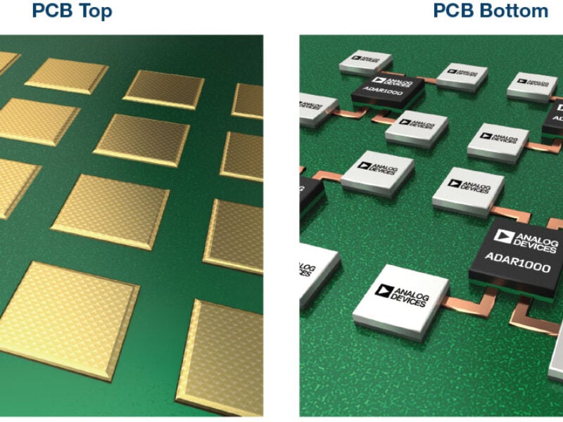
As we construct the entire antenna, there are many challenges of the array design, including the routing of control lines, power supply management, pulsed circuitry, thermal management, environmental considerations, etc. There is a major push in the industry toward low profile arrays that consume less volume and weight. The traditional plank architecture uses small PCB planks with electronics on them perpendicularly fed into the backside of the antenna PCB. This approach has been improved over the past 20 years to continually reduce the size of the plank thereby reducing the depth of the antenna. Next-generation designs move from this plank architecture to a flat panel approach where there is enough integration in each IC to fit them simply on the backside of the antenna board, significantly reducing the depth of the antenna and making them easier to fit into portable or airborne applications. In Figure 3, the image on the left shows the gold patch antenna elements on the topside of the PCB and the image on the right shows the analog front end of the antenna on the bottom side of the PCB. This is only a subset of the antenna where there could be a frequency conversion stage occurring in one end of the antenna, for example, and a distribution network to route from a single RF input to the entire array. It can easily be seen that more integrated ICs significantly reduce the challenges in the antenna design and, as the antennas become smaller with more electronics packed into a reduced footprint, the antenna design demands new semiconductor technology to help make the solutions viable.

Digital beamforming versus analog beamforming
Most phased array antennas that have been designed in past years have used analog beamforming where the phase adjustment is done at RF or IF frequencies and there is one set of data converters for the entire antenna. There is increased interest in digital beamforming where there is one set of data converters per antenna element and the phase adjustment is done digitally in the FPGA or some data converters. There are many benefits to digital beamforming starting with the ability to transmit many beams easily or even change the number of beams almost instantly. This remarkable flexibility is attractive in many applications and is driving its adoption. Continuous improvements in the data converters are lowering power dissipation and expanding to higher frequencies where RF sampling at the L-band and S-band are making this technology a reality in radar systems. There are multiple considerations to make when considering analog versus digital beamforming, but the analysis usually is driven by the number of beams required, power dissipation, and cost targets. The digital beamforming approach typically has higher power dissipation with a data converter per element but offers a lot of flexibility in the ease of creating multiple beams. The data converters also require higher dynamic range since the beamforming that rejects blockers is only done after the digitization. Analog beamforming can support multiple beams but requires an additional phase adjustment channel per beam. For example, to create a 100 beam system would multiply the number of RF phase shifters for a 1 beam system by 100, so the cost consideration of data converters versus phase adjustment ICs can change depending on the number of beams. Similarly, the power dissipation is usually lower for an analog beamforming approach that can utilize passive phase shifters but as the number of beams increases, the power dissipation will increase as well if additional gain stages are needed to drive the distribution network. A common compromise is a hybrid beamforming approach where there are subarrays of analog beamforming followed by some digital combination of the subarray signals. This is an area of growing interest in the industry and will continue to evolve in the years to come.
Semiconductor technology
A standard pulsed radar system transmits a signal that can reflect off an object while the radar waits for the return pulse to map the field of view of the antenna. In past years, this antenna front-end solution would have discrete components, likely based in gallium arsenide technology. The IC components used as the building blocks for these phased array antennas are shown in Figure 4. They consist of a phase shifter to adjust the phase of each antenna element (which ultimately steers the antenna), an attenuator that can taper the beam, a power amplifier used for transmitting a signal, and a low noise amplifier used to receive a signal, as well as a switch to toggle between transmit and receive. In past implementations, each of these ICs could be housed in a 5 mm × 5 mm package, or more advanced solutions could have an integrated monolithic single-channel GaAs IC to achieve this functionality.

The recent proliferation of phased array antennas has been aided by semiconductor technology. The advanced nodes in SiGe BiCMOS, SOI (silicon-on-insulator), and bulk CMOS have combined digital circuitry to control the steering in the array, as well as the RF signal path to achieve the phase, and amplitude adjustment into a single IC. It’s possible today to achieve multichannel beamforming ICs that adjust gain and phase in a 4-channel configuration with up to 32 channels aimed at millimeter wave designs. In some lower power examples, a silicon-based IC could be a monolithic solution for all functions above. In high power applications, gallium nitride-based power amplifiers have significantly increased the power density to fit into the unit cell of phased array antennas that would have been traditionally served by traveling wave tube (TWT)-based PAs or relatively low power GaAs-based PAs. In airborne applications, we are seeing a trend to flat panel architectures with the power added efficiency (PAE) benefits of GaN technology. GaN has also enabled large ground-based radars to move to phased array-based antenna technology from a dish antenna driven by a TWT. We are now able to have monolithic GaN ICs capable of delivering over 100 watts of power with over 50% PAE. Combining this level of PAE with the low duty cycle of radar applications size, weight, and cost of the antenna array. The additional benefit beyond the pure power capability of GaN is the size reduction compared to existing GaAs IC solutions. Comparing a 6 W to 8 W GaAs power amplifier at X-band to a GaN-based solution reduces the footprint by 50% or more. This footprint reduction is significant when trying to fit these electronics into the unit cell of a phased array antenna.
Analog Devices analog phased array ICs
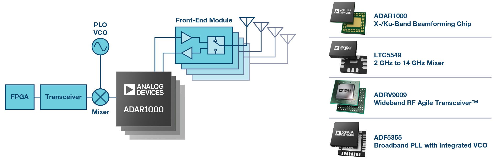
Analog Devices has developed integrated analog beamforming ICs aimed at supporting a range of applications including radar, satellite communications, and 5G telecommunication. The ADAR1000 X-/Ku-band beamforming IC is a 4-channel device covering 8 GHz to 16 GHz operating in time division duplex (TDD) mode with the transmitter and receiver integrated into one IC. This is ideal for X-band radar applications as well as Ku-band satcom, where the IC can be configured to operate in transceiver-only or receiver-only mode. The 4-channel IC is housed in a 7 mm × 7 mm QFN surface-mount package for easy integration into flat panel arrays dissipating only 240 mW/channel in transmit mode and 160 mW/channel in receive mode. The transceiver and receiver channels are brought directly, externally designed to mate with a front-end module (FEM) that Analog Devices offers. Figure 5 shows the gain and phase control with full 360 phase coverage where phase steps less than 2.8° are possible, as well as better than 31 dB of gain control. The ADAR1000 contains on-chip memory to store up to 121 beam states where one state contains all phase and gain settings for the entire IC. The transmitter delivers an approximately 19 dB gain with 15 dBm of saturated power where the receive gain is approximately 14 dB. Another key metric is the phase change over gain control, which is approximately 3° over 20 dB of range. Similarly, the gain change with phase control is about 0.25 dB over the entire 360° phase coverage, easing the calibration challenges.

This beamforming IC is developed for analog phased array applications or hybrid array architectures that combine some digital beamforming with analog beamforming. Analog Devices offers a complete solution from antenna to bits, including the data converters, frequency conversion, and analog beamforming IC, as well as the front-end module. The combined chipset allows Analog Devices to combine functionality and optimize the ICs appropriately to more easily implement an antenna design for our customers.
About the author
Keith Benson graduated from the University of Massachusetts, Amherst with a B.S.E.E. in 2002 and from the University of California, Santa Barbara with an M.S.E.E. in 2004. He spent much of his early career at Hittite Microwave designing ICs used in RF wireless electronics. He then moved to manage a team of IC design engineers focusing on wireless communication links. In 2014, Hittite Microwave was acquired by Analog Devices where Keith became a product line director for RF/microwave amplifiers and phased array ICs. Keith currently holds three U.S. patents related to novel amplifier techniques.
 If you enjoyed this article, you will like the following ones: don't miss them by subscribing to :