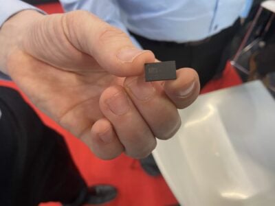
Samsung launches 8nm RF process for 5G chips
Samsung Electronics has launched an 8nm process technology for 5G RF designs with a new transistor design that gives a 35 percent reduction in size and power consumption.
This 8nm process node will enable single chip designs for 5G communications with support for multi-channel and multi-antenna chip designs in the sub-6-GHz and millimetre wave frequency bands. Current RF designs are currently built on 28nm and 14nm processes and the company has shipped 500 million mobile RF chips for premium smartphones since 2017.
“Through excellence in innovation and process manufacturing, we’ve reinforced our next-generation wireless communication offerings,” said Hyung Jin Lee, Master of Foundry Technology Development Team at Samsung Electronics. “As 5G mmWave expands, Samsung’s 8nm RF will be a great solution for customers looking for long battery life and excellent signal quality on compact mobile devices.”
To overcome the challenges of scaling 5G RF and analogue designs, Samsung says it has developed a unique transistor architecture for 8nm that it called RFextremeFET (RFeFET). This provides a 35 percent increase in power efficiency with a 35 percent decrease in the RF chip area compared to the 14nm process.
This provides comparable scaling to digital transistors to enable single chip designs, says Samsung.
Last week rival foundry TSMC announced a 6nm RF process called N6RF aimed at 5G RF transceivers for both sub-6 gigahertz and millimetre wave designs as well as WiFi6E. This is the next step from the current 16nm RF process at TSMC.
 If you enjoyed this article, you will like the following ones: don't miss them by subscribing to :
eeNews on Google News


